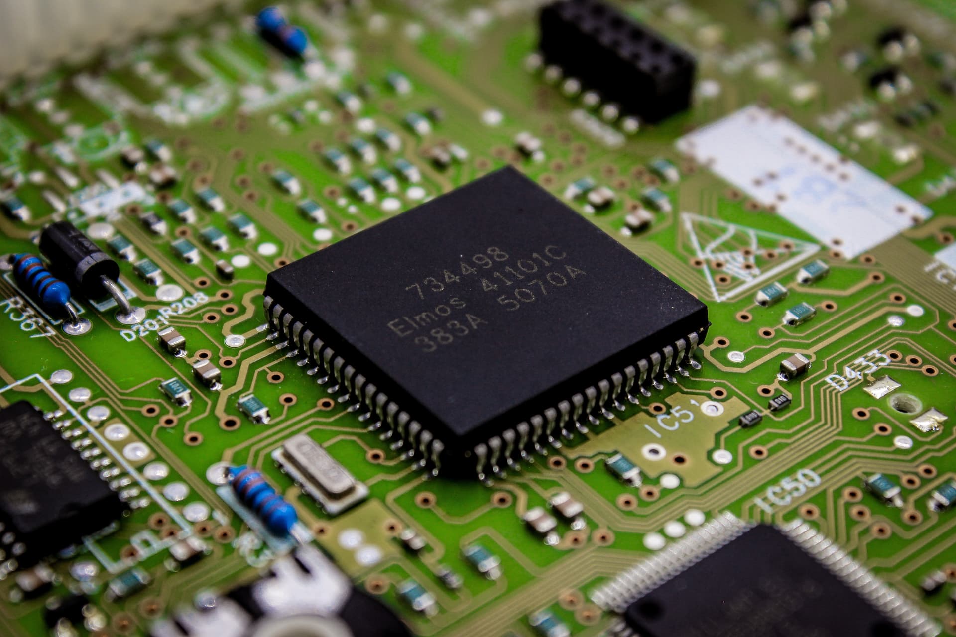
Semiconductor CNC Machining in Singapore
High-precision components and tooling for front-end wafer fabrication and back-end packaging equipment. Sourced and machined in Singapore, Shine provides ±0.01mm critical tolerances, vacuum-grade surface finishes, and certified ISO Class 6 to Class 8 cleanroom cleaning and assembly.
- Critical featuresView detail →±0.01 mm
- Sealing facesView detail →Ra 0.2 µm
- AssemblyView detail →ISO Class 6 cleanroom
- PackagingView detail →Cleanroom double bag
- QualityView detail →ISO 9001:2015
Vacuum Integrity & Contamination Control
Semiconductor fabrication equipment demands strict control over particle generation, outgassing, and chemical compatibility. We manufacture components with controlled surface roughness down to Ra 0.2µm, precise seal groove geometries, DI water ultrasonic cleaning, and cleanroom double-bagging to protect wafer processing environments.
- Precision tolerances - Down to ±0.01mm on critical alignment features, wafer stages, and chucks
- Cleanroom packaging - ISO Class 6, 7, and 8 controlled cleanrooms for ultrasonic DI cleaning, mechanical sub-assembly, and ESD double-bagging
- Vacuum & plasma compatibility - Validated materials and surface treatments for high-vacuum and corrosive gas environments
- Multi-axis capability - Simultaneous 5-axis CNC milling for complex fluid manifolds, showerheads, and vacuum chambers
- Production milling & turning - 3- and 4-axis CNC milling for chamber lids, base plates and liner plates, and CNC turning for vacuum flanges, spindles and nozzles
For an in-depth specifier's guide on preventing particle shed, vacuum outgassing, and chemical attack on engineering drawings, read our guide on CNC Machining for Semiconductor Equipment: What to Specify and Why.
Semiconductor Applications
- Process chamber components - Vacuum flanges, chamber lids, liner plates, and gas distribution showerheads
- Wafer handling & transfer - Robotic end-effectors, vacuum chucks, transfer arms, and alignment nests
- Gas & liquid delivery manifolds - High-purity fluid blocks, valve bodies, and leak-tight gas delivery channels
- Test & burn-in sockets - High-density probe plates, guide plates, and insulating carriers in engineering plastics and FR4
- Optical & metrology stages - Low thermal expansion brackets, sensor mounts, and interferometer stages
Materials for Semiconductor Equipment
We machine certified high-purity metals and engineering plastics tailored to specific fab process requirements:
- Aluminium (6061-T6, 7075-T6) - Vacuum chambers, robot arms, and base plates finished with clear or hardcoat anodizing
- Stainless steel (316L, 304L) - Vacuum manifolds, gas delivery lines, and corrosive fluid components with optional electropolishing
- PEEK (Unfilled, Ceramic-filled) - Dimensionally stable, chemically resistant wafer contact parts, chucks, and high-voltage insulators
- PEI (Ultem 1000/2300) - High-temperature test sockets, probe heads, and structural dielectric insulators
- PTFE and Polypropylene - Wet bench components, chemical bath tanks, and inert fluid routing
- FR4 / G-10 - High-rigidity insulating backer boards and semiconductor test fixtures
- Invar 36 - Ultra-low thermal expansion mounting plates for laser lithography and metrology systems
Cleanroom Assembly & Packaging Protocols
Components requiring high cleanliness undergo multi-stage ultrasonic degreasing and deionized water rinsing before entering our certified cleanrooms. Sub-assemblies are completed in ISO Class 6 or Class 7 environments, vacuum-sealed in cleanroom-grade antistatic polyethylene bags, and double-bagged for direct introduction into customer clean environments without additional on-site cleaning loops.
Why Semiconductor Equipment OEMs Partner with Shine
- Integrated Cleanroom Workflow - In-house ISO Class 6, 7, and 8 cleanrooms for ultrasonic DI water washing, mechanical sub-assembly, and cleanroom double-bag packaging.
- Vacuum-Grade Surface Finishes - Sealing faces machined to Ra 0.2 µm with controlled O-ring gland geometries and verified leak-tightness.
- Fab-Proven Materials - Decades of machining experience across certified 6061-T6, 316L, virgin/ceramic-filled PEEK, PEI Ultem, and PTFE.
- Lot-by-Lot Metrology Verification - Zeiss CMM reports, SmartScope vision measurement logs, and material test certificates delivered with every shipment.
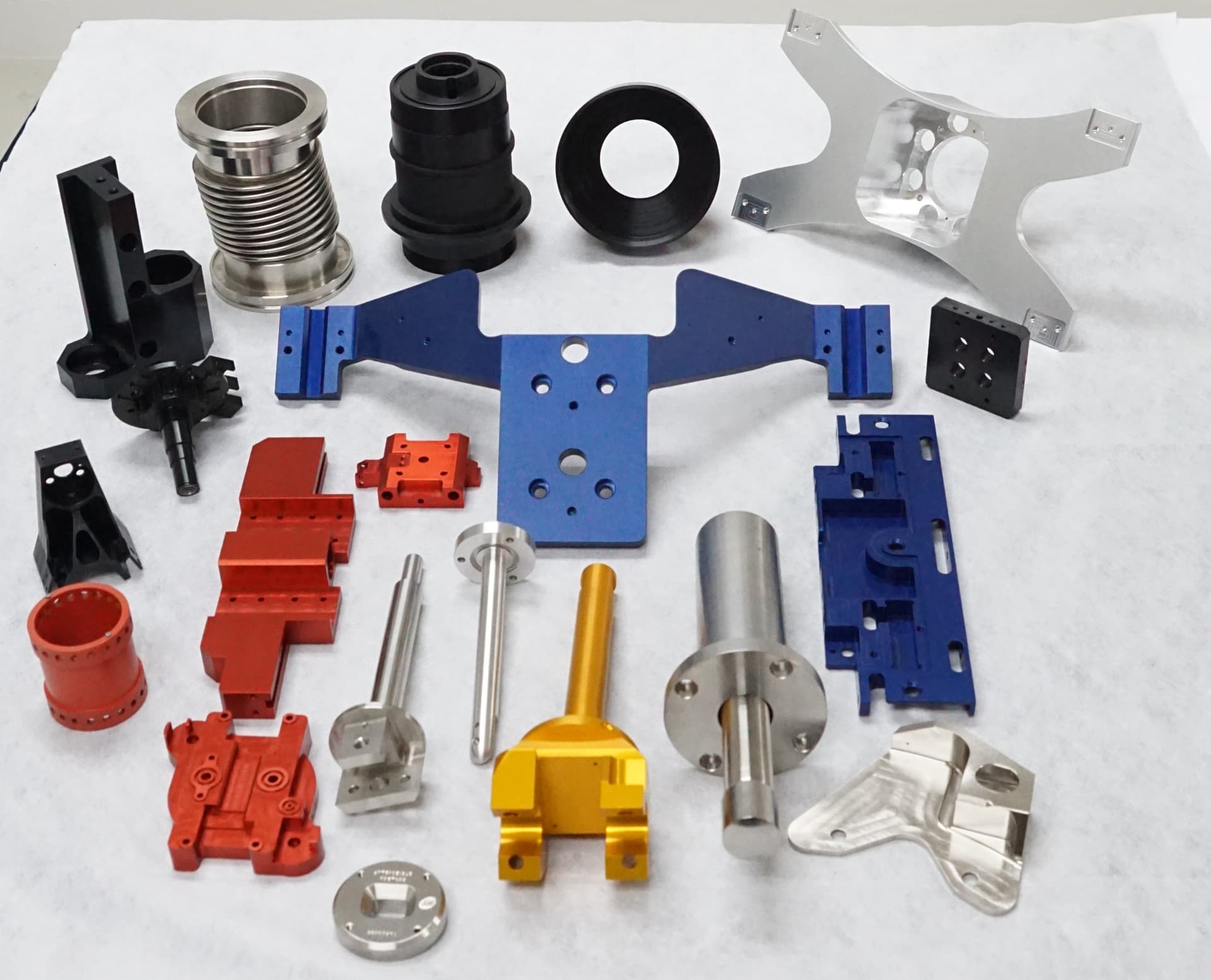
Semiconductor Parts Gallery
Sample parts produced at our Singapore facility for this sector:
Quality Documentation Delivered With Every Lot
Semiconductor equipment lots ship with the standard records plus the cleanliness evidence a fab tool maker needs:
First Article Inspection (FAI)
Setup approval measured on Zeiss CMM before a production run is released.
Dimensional inspection report
100% or AQL sampling report against the drawing, per customer inspection plan.
Mill Test Certificate (MTC)
Raw material chemistry and mechanical properties, traceable to the lot.
Certificate of Conformance (CoC)
Issued with every shipment under the ISO 9001:2015 quality system.
Cleaning & packaging record
Ultrasonic DI cleaning batch, particulate spot audit, and cleanroom bag lot per part or module.
Surface treatment certificate
Coating type and thickness for anodized, electroless nickel or electropolished vacuum parts.
Metrology equipment, calibration schedules, and complete inspection workflows are detailed under quality & compliance.
Semiconductor Component Engineering Review & RFQ
Connect directly with our Singapore engineering team for technical feasibility evaluation, DFM analysis, and itemized quotation within 24 to 48 hours:
Technical Package Specifications
- 2D drawing with vacuum-facing surface roughness (Ra) callouts & 3D CAD model
- Cleanliness & cleanroom packaging requirements (ISO Class 6/7, double bagging)
- Process-gas or plasma exposure conditions for material & coating compatibility
Deliverables Provided (24–48 Hours)
- Itemized quotation with unit and batch pricing and confirmed delivery schedule
- Engineering DFM analysis (fixturing, tolerances, and cost optimization recommendations)
- Quality inspection plan proposal (Zeiss CMM metrology reporting, FAI scope)
Frequently Asked Questions
What tolerances can you hold on semiconductor components?
We achieve tolerances down to ±0.01mm on critical mounting faces, dowel pin locations, and wafer nesting features. Full CMM inspection reports are provided with each delivery.
How are parts cleaned and prepared for cleanroom delivery?
Parts pass through automated ultrasonic cleaning with deionized water, followed by hot air drying. Final assembly, inspection, and vacuum double-bagging take place in our ISO Class 6 and Class 7 cleanrooms.
What surface treatments are available for vacuum and plasma environments?
We provide Class 100 compatible Type II and Type III hardcoat anodizing, chemical conversion coating (Alodine), electropolishing, and passivation through controlled, certified finishing lines.
Can you machine complex engineering plastics like PEEK and Ultem without warping?
Yes. We use specialized tooling geometries, proper coolant management, and intermediate stress-relieving heat treatments to ensure tight dimensional stability on high-performance plastics.
Explore Other Manufacturing Services
All services →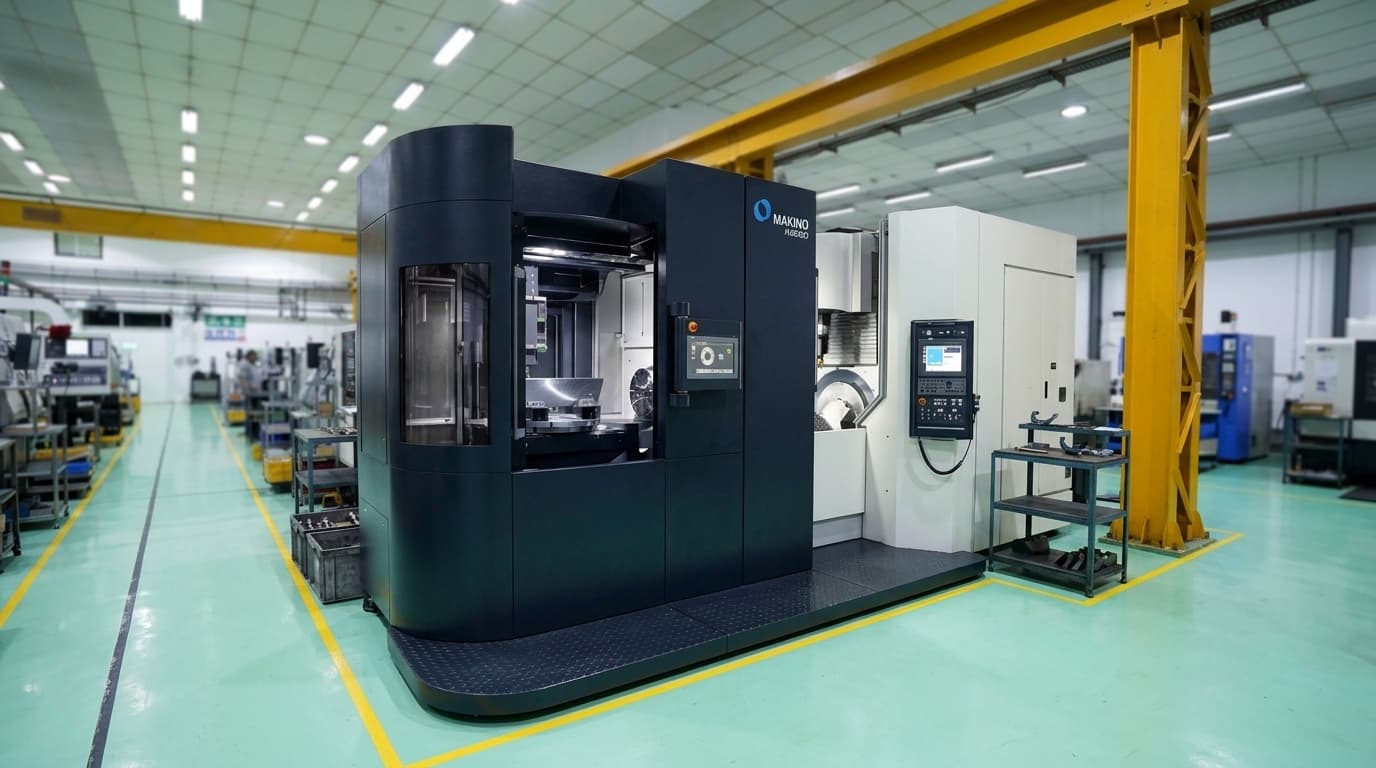
5-Axis CNC Machining
Simultaneous 5-axis milling for complex 3D contoured parts and tight tolerances to ±0.010mm.
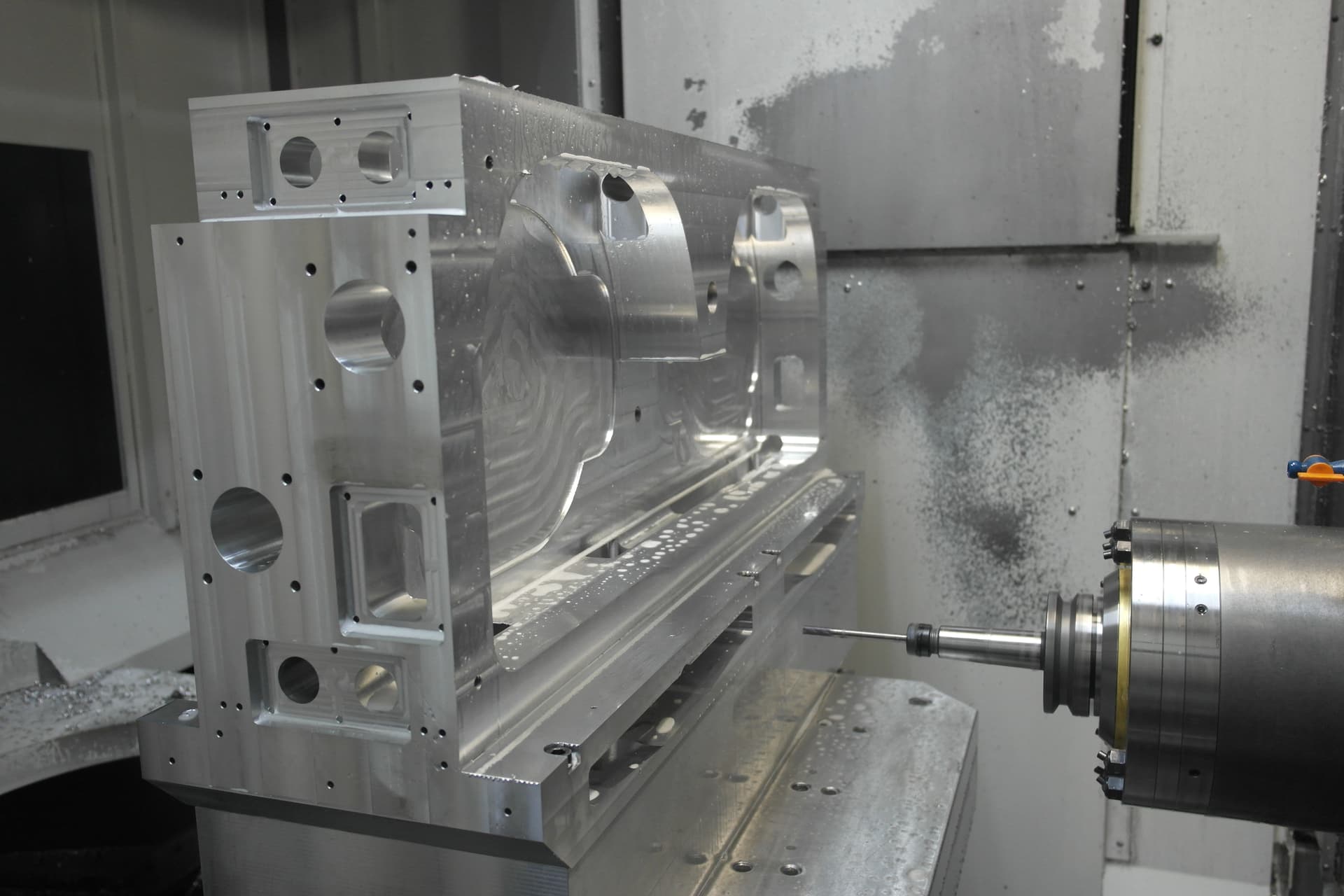
CNC Milling
High-speed 3- & 4-axis milling for prismatic enclosures, cold plates, and precision brackets.
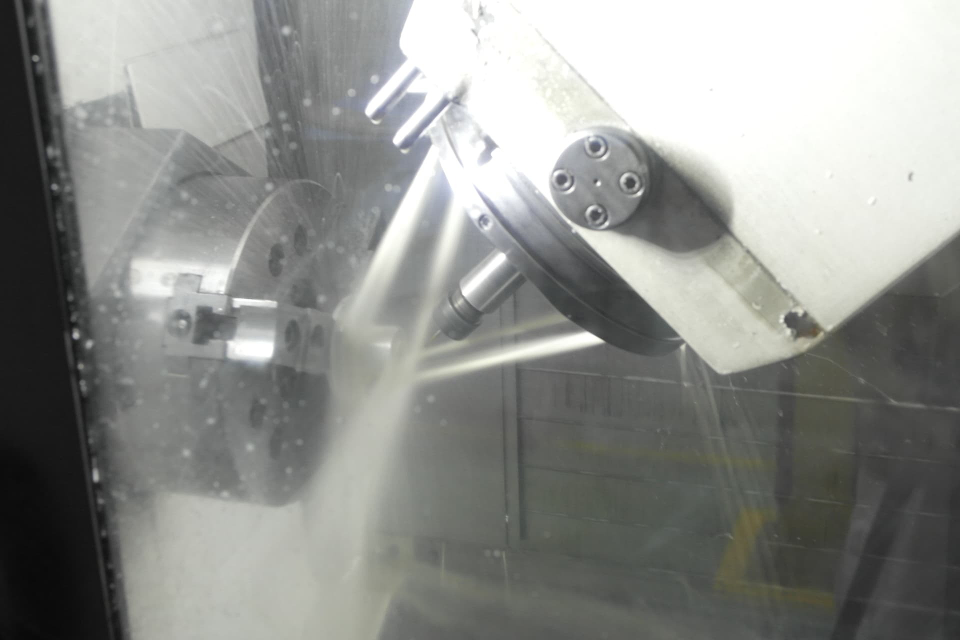
CNC Turning
Multi-axis live-tooled turning for shafts, cylinders, and rotational parts up to 650mm diameter.
Surface Finishing & Anodizing
Managed Type II/III anodizing, Alodine, electroless nickel plating & passivation with CAM coating allowances.
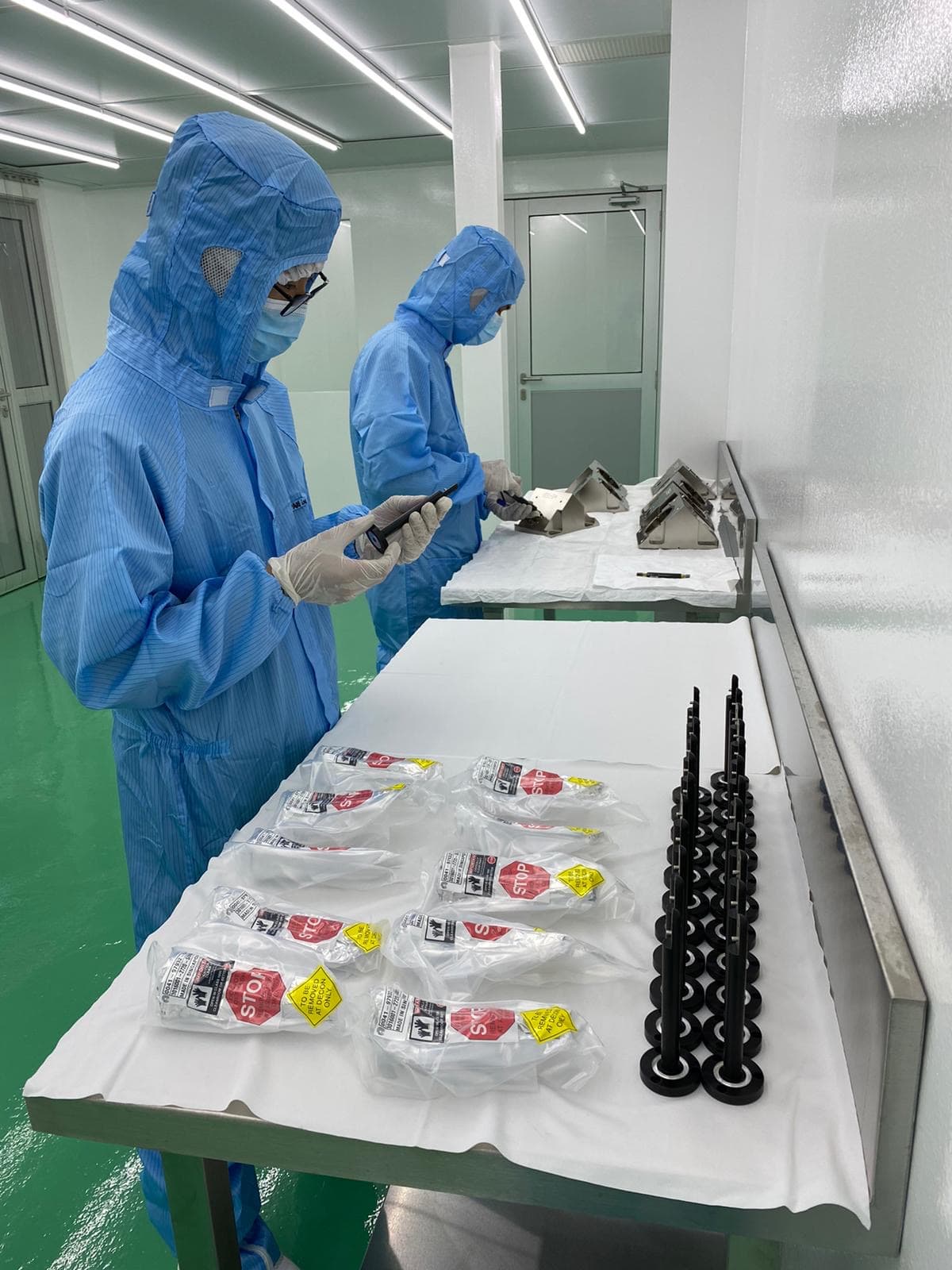
Cleanroom Assembly
ISO Class 6–8 cleanroom mechanical assembly, ultrasonic DI water cleaning, and ESD double-bagging.
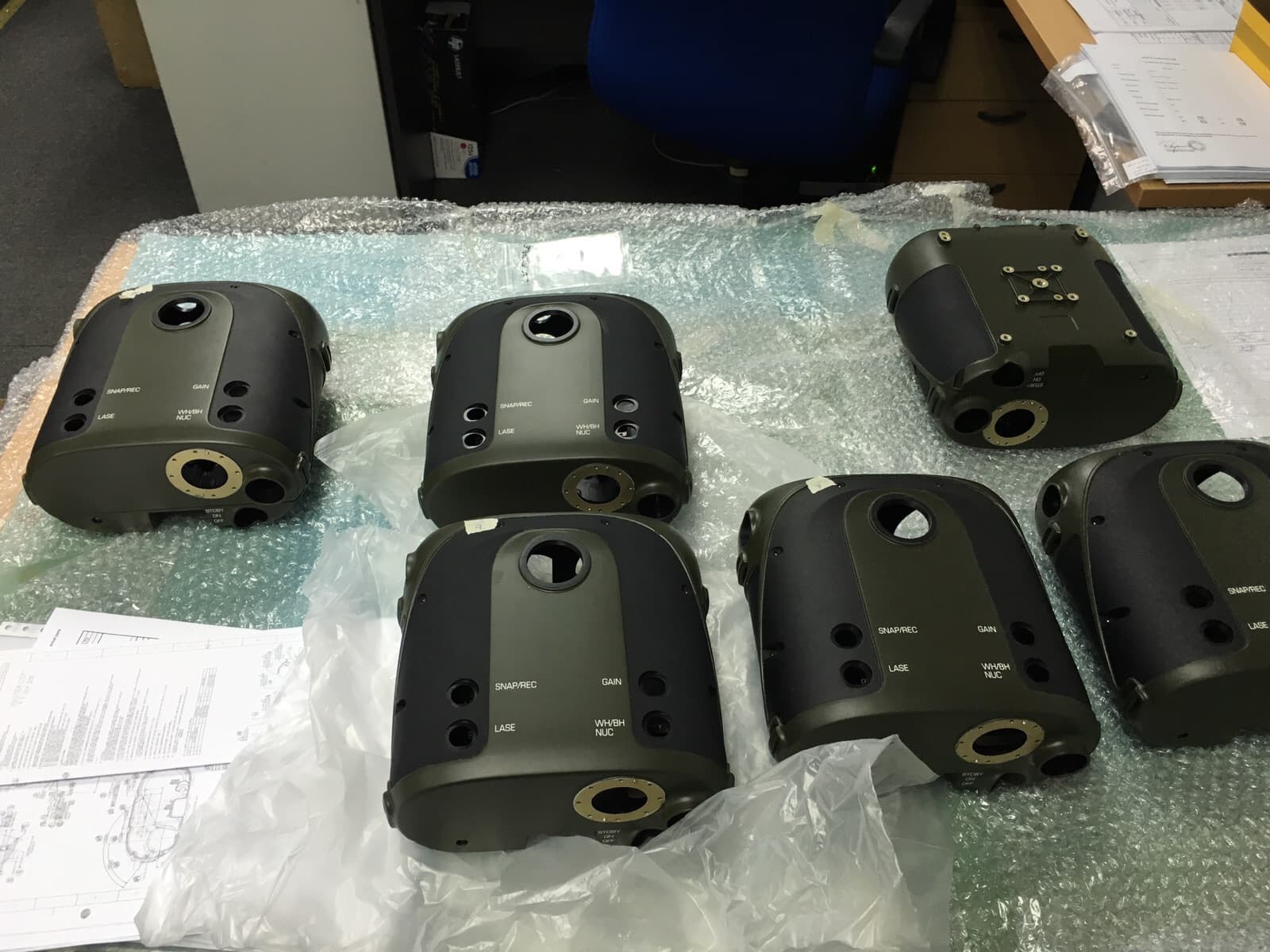
Turnkey Contract Manufacturing
Single-source contract manufacturing managing BOM sourcing, machining, assembly, and testing.
Other Industries We Serve
All industries →
Medical
Precision surgical instruments, orthopedic trial components & diagnostic fluidic manifolds.

Optics & Photonics
High-stability Invar 36 laser benches, threaded lens barrels & optical mounts.

Automotive & EV
EV battery cooling plates, high-conductivity busbars & powertrain components.

Oil & Gas
Severe-service valve bodies, downhole sensor housings & subsea connectors.
Speak with Our Semiconductor Machining Specialists
Connect with our Singapore engineering team for vacuum chamber, manifold, or tooling review, cleanroom packaging scoping, and quotation within 24 to 48 hours.
- Mutual NDA executed within 24 hours
- ISO 9001:2015 certified & Cyber Essentials mark
- 24–48h engineering DFM feedback & formal RFQ pricing